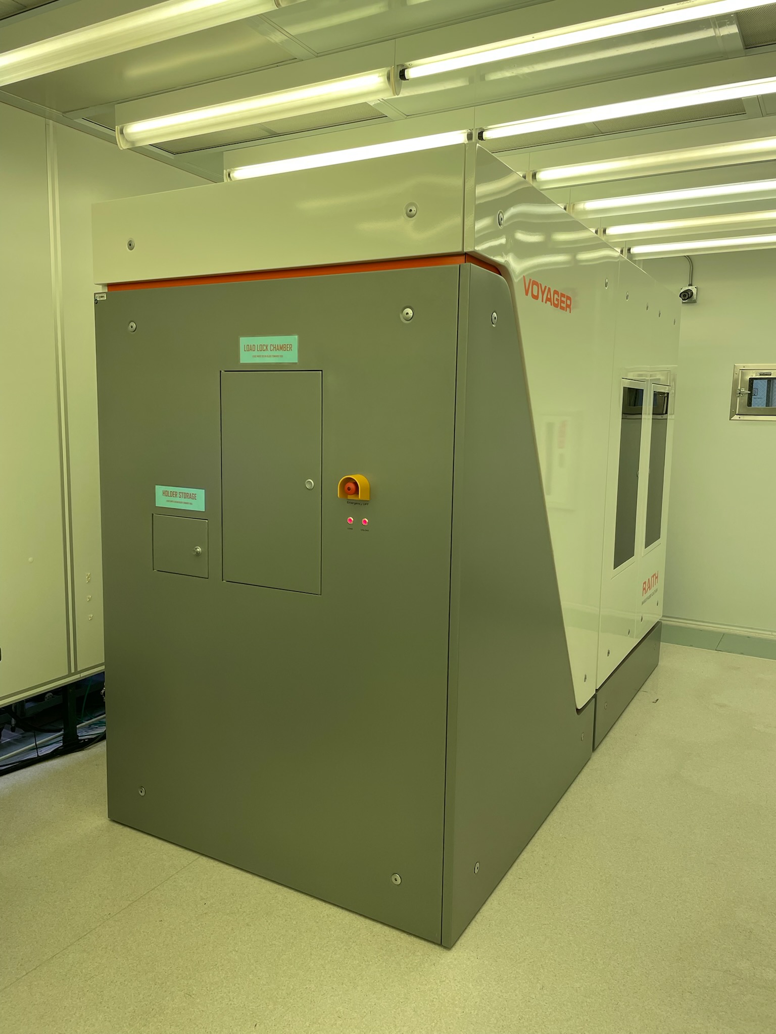
Fully automated 50 kV electron beam lithography with sub-20 nm overlay and high-throughput exposures is online and ready for users.
Start the process to gain access to UNM NanoFab cleanroom facilities, training resources, and fabrication equipment.
Learn more about the Center for High Technology Materials, its research programs, faculty, and additional research facilities.

Fully automated 50 kV electron beam lithography with sub-20 nm overlay and high-throughput exposures is online and ready for users.
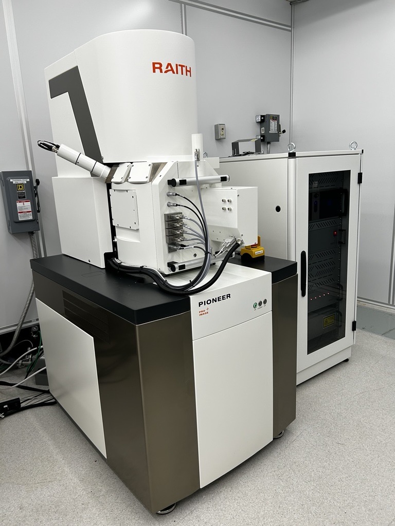
Integrated SEM analytics with professional-grade EBL (1.6 nm min beam size) enables write-and-verify workflows without sample transfer.

Quantum Design (QD), the manufacturer of UNM NanoFab's MPMS (Magnetic Property Measurement System), will hold a two-day in-person workshop at CHTM.
Click the event to read and learn more about the talk.
Our latest publication explores cutting-edge semiconductor fabrication techniques that improve efficiency and reduce waste.
A new study from our facility outlines improved safety protocols that have been adopted across multiple research labs.




© The University of New Mexico
Albuquerque, NM 87131, (505) 277-0111
New Mexico's Flagship University