RAITH VOYAGER - EBL


Overview
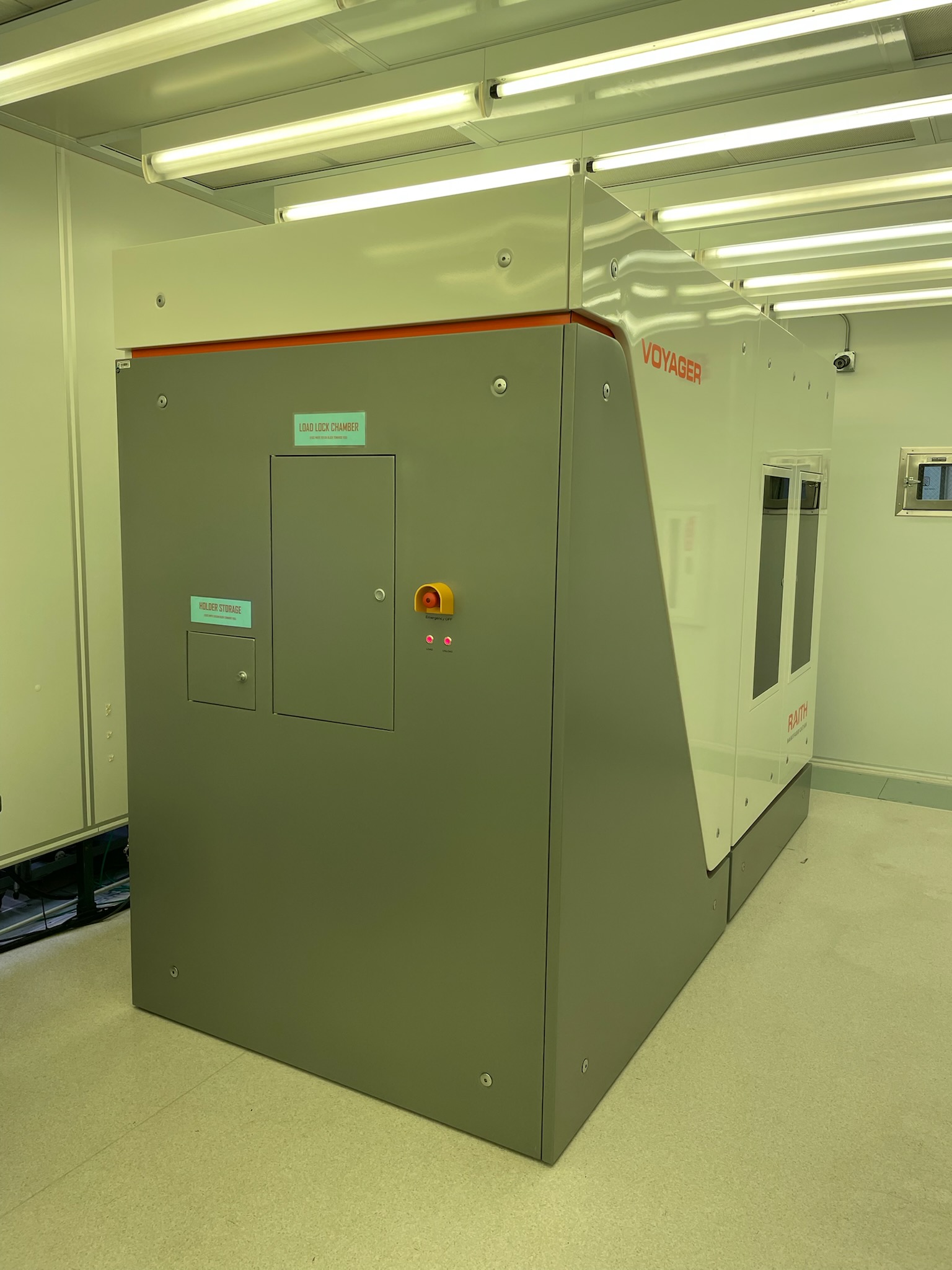
EBL (electron beam lithography) is a unique process of forming patterns on a chip/substrate. The Raith VOYAGER is a cutting-edge, fully automated electron beam lithography system designed to deliver the highest performance nanofabrication for advanced research and development applications. Built for precision, automation, and exceptional throughput, it is ideal for creating photonic devices, high-frequency electronics, quantum structures, and nanostructures with unprecedented ease of use.
The tool provides automated workflows and comprehensive system control, ensuring consistent results with minimal user intervention. The tool features a 50 kV electron beam with fully automated real-time corrections, overlay accuracy better than 20 nm, field stitching accuracy better than 20 nm, exceptional exposure speeds reaching sub 2 hours per square centimeter for high-density gratings, and a sophisticated 20-bit FPGA-based pattern generator with 500 µm write field capability. The advanced deflection system incorporates real-time dynamic corrections across the entire write field, and the multi-sample holder supports varied substrate dimensions up to 150 mm wafers.
Automation & Control
The tool provides fully automated laser leveling and alignment for consistent exposure quality across all samples, laser interferometric corrected stage movement enabling continuous stitching on large area patterns without field boundaries, and proprietary eWrite technology with single-stage electrostatic deflection to define ultra-high-resolution patterns. The system incorporates built-in RAITH NANOSUITE software providing comprehensive pattern editing capabilities, and NanoPECS for accurate proximity-effect correction of nanoscale structures with automated parameter optimization.
Advanced Optional Capabilities
Advanced optional capabilities include laser height sensing for automatic sample leveling and focus optimization, traxx stitching-error-free exposure mode for seamless large-area patterning, periodixx technology for ultra-precise periodic structure fabrication with sub-nanometer pitch control, 20-bit pattern generator resolution for maximum precision in complex designs, bitmap patterning exposure module for direct grayscale lithography applications, and sample navigation on image functionality for intuitive sample positioning and pattern placement.
Applications
The applications of such a distinctive automated tool are numerous, including high-resolution photonic integrated circuit fabrication with stitching-error-free waveguides, high-frequency electronic component manufacturing for advanced telecommunications, precision optical component development, advanced metamaterials and photonic crystal research, quantum device prototyping and characterization, large-area nanostructured device production with exceptional uniformity and reproducibility, and direct grayscale lithography for three-dimensional nanostructure fabrication.
